The Amiga 1000 is a slick looking machine. It however loads its ROM from floppy disk. The Wikipedia Article on the Amiga 1000 explains why.
I wanted to put a Kickstart 1.3 ROM in my Amiga 1000. There are adapters out there you can build and install. I chose one, followed the instructions, and it didn't work.
After a whole lot of digging I finally got it working and now I'm documenting what hilarity I found.
I started with this one from the amiga community. The PCB manufacturing files are available on PCBWAY as a shared project. So, I got the board made, did the board mods on my Amiga 1000, and set it up. No bueno.
Let's go over the mods first before I explain why it didn't work.
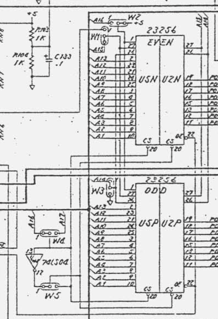
First up, the Amiga 1000 has a pair of small ROMs (lower and upper 8 bits of the data bus) to bootstrap the ROM image from floppy disk, throw it into the write once memory store and then kick it appropriately to take over the ROM memory address range. The ROM address range is $F80000 -> $FFFFFF - a 512KiB region. But, this ROM isn't that big at all.
The schematic calls out what's going on pretty clearly. This is for the early revision Amiga 1000, with the U5N / U5P ROMs populated.
The /OE lines (pin 22) go to /ROM01 on the PALs, which (among other things) enables the ROMs only when the write-once memory store isn't active and we're in the ROM region.
But look at the other bits going on.
First, pin 1 is going to +5 volts, instead of A16. Pin 27 is going to A15 instead of .. the processor R/W pin? Weird. Anyway, let's look at these ROMs.
First confusing thing here - the ROMs addressing starts from A0 to A14. The 68000 bus however doesn't have an A0 - it's A1 to A23, and then there's upper/lower byte select lines. So, this ROM A0 is the CPU bus A1, the ROM A1 is CPU bus A2, etc.
Pin 1 is NC - it'd be ROM A15 on a 64k x 8 ROM. Ie, Amiga/68000 A16. And pin 27 is ROM 14, Amiga/68000 A15. That makes sense.
What's happening with the OTHER /CS line though?
On U5N/U2N, the /CS2 lines in the schematic to go W2 and W5. The intention looks to be whether A16 or A17 acts as a chip select line to enable either the lower or upper set of ROMs. If you wanted 32KiB ROMs then you'd want A16 to be the /CS2 control. If you wanted 64KiB ROMs then you'd want A17 to be the /CS2 control.
In theory, if everything is wired up fine, this means you can fit 256KiB of ROMs by fitting four 64KiB ROMs and jumpering things appropriately. You'd want:
- W2 to be CPU A16
- W1 to be CPU A15
- W3 to be CPU A14
- W4 to be CPU A17
- W5 to go via the 74LS04 to invert A17 as the /CS2 line, so either the U5N/U5P is enabled, or the U2N/U2P is enabled.
However, this just plainly didn't match what's on my board. After trying a couple times to do the whole mod, I started to question whether the PCB matched the schematic. Hint, it ... didn't.
Here's what the PCB layout looks like, front:
and back:
You can see where you need to cut W1, W2, W3, W4 (and W5, but I didn't) to turn it into a selectable jumper set.
So, I buzzed out both the ROM board and the Amiga 1000 board to see what was going on. And what I found was ... pretty amusing. I removed all four jumpers and:
- 68000 D0..D15 are OK
- 68000 A1..A15 are OK
- 68000 A16, A17 - not OK!
- 68000 A18 - OK!
The A18 line made it to the ROM board via one of the wires soldered to the write-once RAM board. The ROM /CS line was soldered to the write-once RAM board as well.
Then I went digging on the ROM board. Let's use ROM numbering now, starting at A0 (cause that's how my notes went.) A0 to A8, A9, A10, A11, A13 used the "even" ROM address lines. A15 used pin 1 on the odd side. A16 on the kickstart ROM mapped to /CS2 on the odd side. A17 on the kickstart ROM mapped to the 4 pin connector and over to the write-once memory board. Same with the ROM /CS line.
So, I had some culprits.
- /CS2 maps to ROM A16 which is Amiga/68000 A17. Ok, so maybe I can play with that on the Amiga side using W4, right?
- Where the heck was Amiga/68000 A16 being routed?
- ROM A15 on odd pin 1 should be controlled by W2, either being Amiga/68000 A16, or +5v, right?
Ok, so then I started buzzing the jumpers and finding out where they went. I then made my first discovery - the trace to ROM /CS2 ? It was tied to CPU A16. No matter what. So, I couldn't flip W4 to the alternate configuration - that shorted ROM /CS2 and CPU A16 to CPU A17. Which means I could not use the /CS2 pin on the ROM adapter, I had to run a separate wire to connect it to CPU A17 and have it end up on the right ROM pin!
Ok, so. I did that. I routed ROM A16 to the middle pin of W4 and ROM A17 to the right hand pin of W4. The rest of the jumpers mirrored the original configuration of the Amiga 1000.
.. but then, nothing. Ok. I went looking at what else could be missing. Then I found the fun reason - the kickstart adapter PCB didn't at all hook up the /BYTE control line to anything. It was just floating. This is problematic for things like DiagROM or the flash based ROM replacements which expect /BYTE to be set correctly for word access. So, I soldered a wire to +5v so it would be tied high and enable word mode.
Success! The ROM booted to a green screen! Ew.
So, in went the
Amiga DiagROM. And DiagROM booted! And gave me a lovely screen of horizontal bars! Now, they're supposed to hint at which data line could be busted, but they were all light green and I was told by the author that it may also be not finding enough chip RAM. He suggested a 5V UART directly attached to the UART TX pin on Paula, and that's what I did.
And he was right - it was only detecting 64k of chip RAM.
I was very confused. I slept on it. The next day I fired up the DiagROM again but with some fast RAM attached, so DiagROM would actually start all the way. Then I used the memory editor to edit regions of chip RAM to see how it behaved. The RAM behaved .. fine? Until I looked a bit closer.
The first 64KiB of chip RAM was mirrored in the second.
The third 64KiB of chip RAM was mirrored in the fourth.
etc.
That told me A16 was stuck. But, it couldn't be the whole of A16, or the ROM code wouldn't get very far. No, it was something to do with RAM. Or, to be clear, the address decoding of chip RAM. I had a late night idea that day- what if the bit wasn't stuck, but it .. wasn't being routed?
So I buzzed the chip RAM address bus, here:
These go up to the write-once memory board, so I buzzed A16 on pin 10 of that chip and ... bam. Nothing. No connection to CPU A16.
Then I buzzed the jumpers. And I found the last thing that super surprised me.
The left hand side of W4, that was connected to the CPU A16 and /CS2 line? That pin goes to the RAM A16 line.
And so does the W2 jumper. The left hand side of W2 is RAM A16. The middle is ROM A16. The right is +5v.
So, the PCB routing seems hella wrong there.
So, after removing two pins from my adapter, routing /CS and A17 directly out as wires for A16 and A17, and hooking them up as shown, DiagROM started and all chip RAM was found. When I flipped out the Diag ROM for a Kickstart 1.3 ROM, it also worked fine.
As you can see, the jumper positions are basically where they were for an unmodified board, except that I'm manually grabbing the Amiga/68000 A16/A17 lines and running them to the ROM adapter (and those pins are removed from both odd/even connectors!)
Well, that was fun. "Fun". I have a second Amiga 1000 here, I may choose a different path for its upgrades.