In a previous post I dumped a bunch of information I had learnt about what had happened in open source Amiga hackery. I've now gone and committed the initial hacks needed to prove that it works and document how I did it.
My goals here were:
- Build one of the memory expansion Gary adapters that are out there - I chose the PeteAU design that I've checked in here;
- Figure out how to modify a rev6 amiga 500 board so I can put 1MB of chip RAM in the provided sockets there (with the schematic available here);
- Make it so a normal A501 512K RAM + RTC add-on can be plugged in to provide the 512k of slow RAM.
First up, it worked. Here's how dirty it is.

The overview is pretty conceptually easy.
- The PeteAU Gary adapter (and I'm sure others!) use the RAS1 line into Agnus and its A19/A23 address line to map RAM into Agnus' other 512k addressable RAM space. The RAM expansions are thus muxed on breaking out CASL and CASU lines whilst enabling RAS1.
- The little break out PCB there is the 74HCT139 dual 2-to-4 demux to decode the two address line bits from the Gary adapter + CASL/CASU lines from Agnus into four CASL/CASU lines.
- The "first" bank from the PeteAU Gary adapter is mapped in as the second half of the 512k chip RAM - and as seen in the picture above, those bent legs are CASL/CASU lines.
- The two tracks that run from U35 out to the trapdoor expansion connector are the CASL/CASU lines to said trapdoor expansion connector. I've cut those and wired them into the second CASL/CASU pair from the 74HCT139 demux.
- No modifications are done on the A501 expansion board.
I've basically just migrated the 74CHT139 from the PeteAU Gary+RAM expansion adapter board back onto the Amiga 500 rev6 PCB.
Here's the relevant bits from the rev6 schematic:
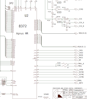

The second bank of 512k chip RAM is U20,U21,U22,U23. It uses RAS1 and the same CASL/CASU that the first bank of 512k chip RAM and the expansion connector.
On the rev6 PCB the CASL/CASU tracks route from U35 to both the RAM and the expansion connector. Cutting the tracks going to the expansion connector is fine; they run there and stop.
Now, finding useful documentation for what to do.
First up, figuring out how to configure the Amiga 500 rev6 PCB.
- J2 (the Agnus A19/A23) jumper was cut so it could be wired into the Gary adapter.
- J7 (the EXP signal from the expansion connector to Gary to say the expansion RAM is there) is left alone, so the A501 can assert it if it's there.

And then how I configured my Gary adapter board:

- JP1 and JP2 set to 2-3 - ie 1M chip
- JP3 set to 1-2 - ie 1.5M slow (decoding all of the space, even if I'm not really decoding stuff from the 74HCT139 to more slow RAM)
- JP4 set to 1-2 (ie, "more slow", so the Gary adapter is properly doing its thing)
And finally, how it looks when it's all done:


(Yes, I was playing with the default colours in the second one, I always disliked the orange.)
I believe it should be 44256 not 41256 (4 bits per chip) as piggyback
ReplyDelete